


MTW European Type Trapezium Mill
Input size:30-50mm
Capacity: 3-50t/h
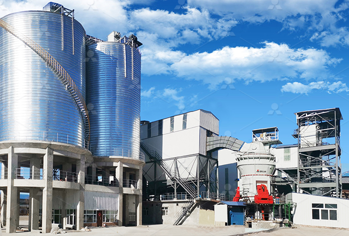
LM Vertical Roller Mill
Input size:38-65mm
Capacity: 13-70t/h
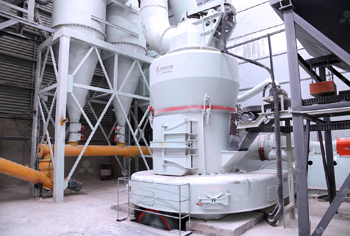
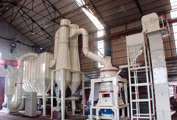
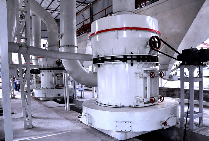
Raymond Mill
Input size:20-30mm
Capacity: 0.8-9.5t/h
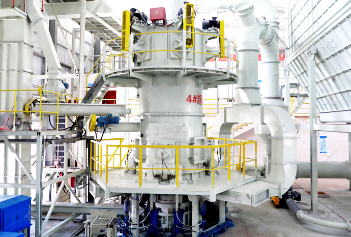
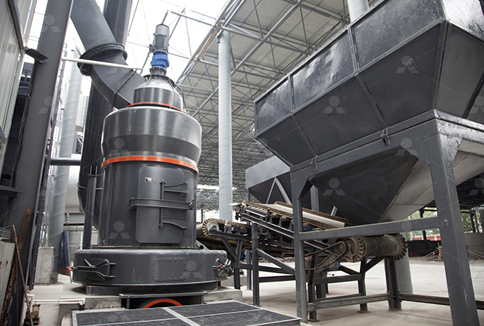
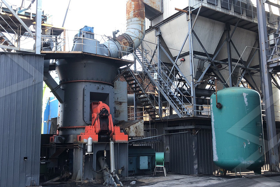
Sand powder vertical mill
Input size:30-55mm
Capacity: 30-900t/h
LUM series superfine vertical roller grinding mill
Input size:10-20mm
Capacity: 5-18t/h
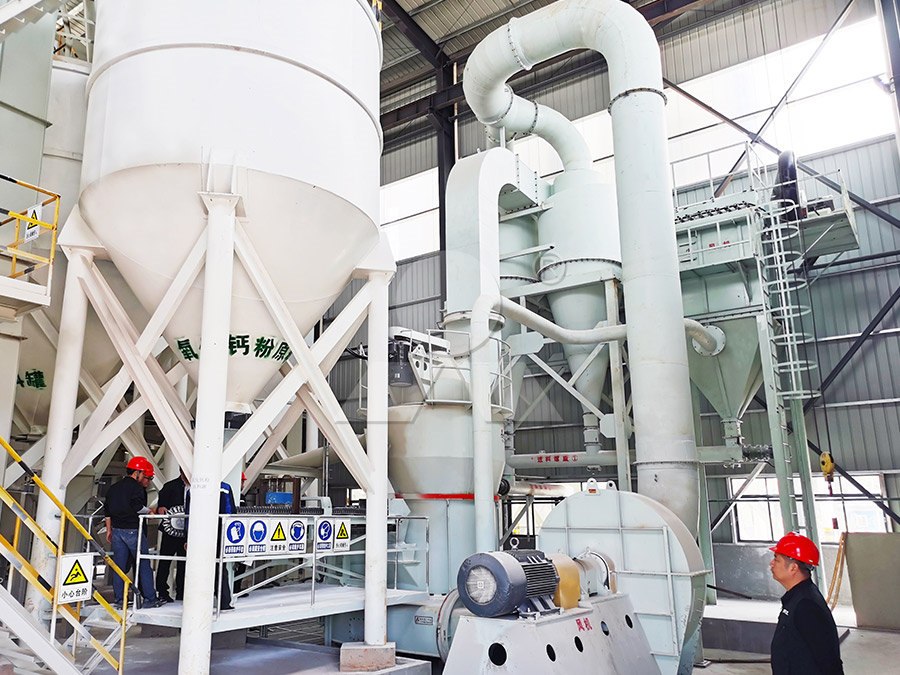
MW Micro Powder Mill
Input size:≤20mm
Capacity: 0.5-12t/h
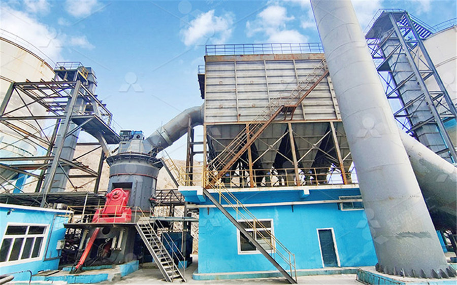
LM Vertical Slag Mill
Input size:38-65mm
Capacity: 7-100t/h
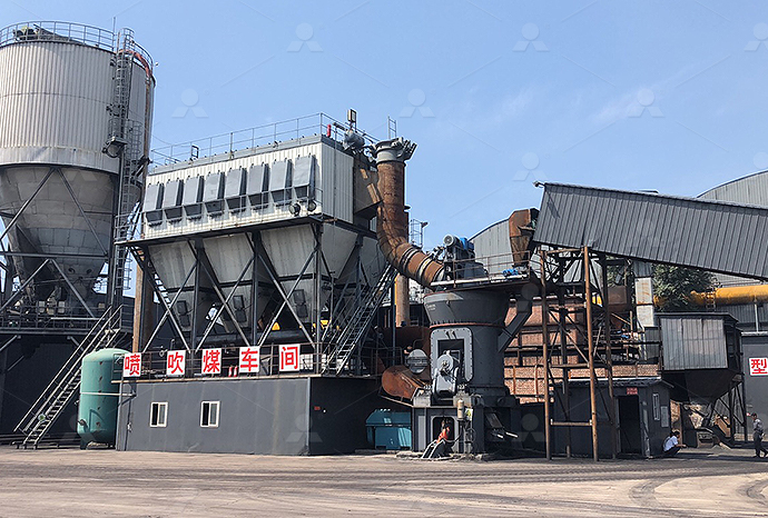
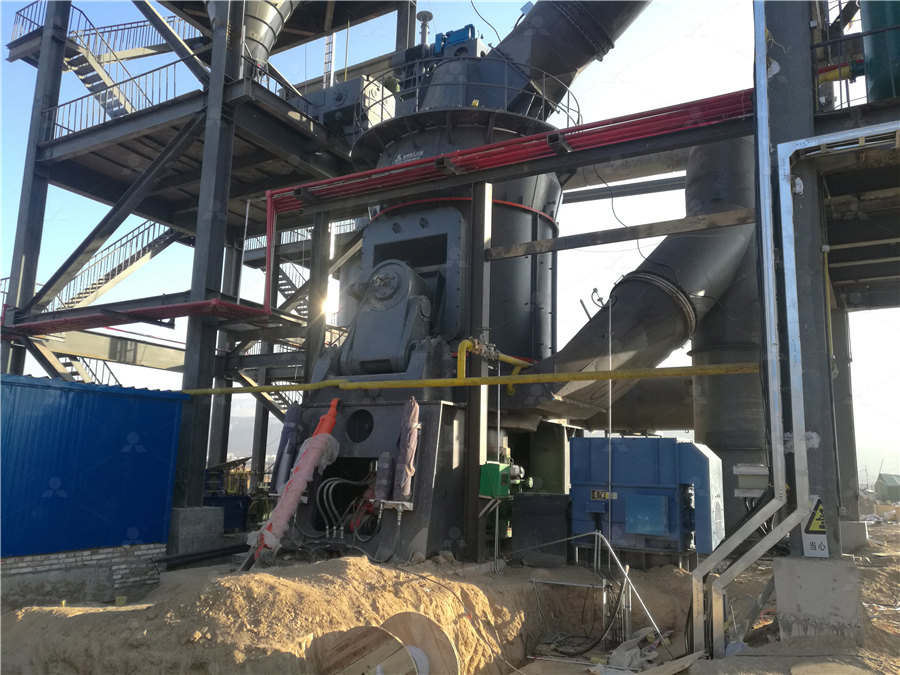
LM Vertical Coal Mill
Input size:≤50mm
Capacity: 5-100t/h
TGM Trapezium Mill
Input size:25-40mm
Capacity: 3-36t/h
MB5X Pendulum Roller Grinding Mill
Input size:25-55mm
Capacity: 4-100t/h
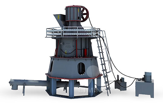
Straight-Through Centrifugal Mill
Input size:30-40mm
Capacity: 15-45t/h
Extracting silicon wafers Extracting silicon wafers Extracting silicon wafers
.jpg)
Extracting bulk defect parameters in silicon wafers using machine
2020年9月18日 To overcome these limitations, this study proposes a machine learning (ML) based approach to extract the defect parameters from lifetime curves MLbased methods are 2022年9月15日 This work proposed ShuffleNetv2 with CNN architecture for silicon wafer defect classification The ShuffleNetv2 performs as a feature extraction model and CNN performs as a classification model This research Classification of Silicon (Si) Wafer Material Defects in 2015年3月30日 Here, we report an aerosolassisted method to extract silicon nanoparticles from such sludge wastes and their use in lithium ion battery applications Using an ultrasonic spray AerosolAssisted Extraction of Silicon Nanoparticles from Wafer 2023年11月28日 This chapter reviews the Si waferprocessing technology, including ingot heat treatment, cutting, slicing, lapping, polishing, wafer cleaning, and packaging The ingot heat Silicon Wafer Processing SpringerLink
.jpg)
Fabrication and characterization of silicononinsulator wafers
2023年11月13日 The Smart Cut™ technology is a layer transfer process that has significantly influenced the silicon wafer industry by facilitating the production of SOI wafers The Smart 2020年1月1日 This chapter discusses the preparation and properties of silicon wafers in detail Microelectromechanical systems (MEMS) manufacturing sets special requirements for silicon Silicon wafers preparation and properties ScienceDirect2020年5月4日 The demand for crystalline silicon wafers is continuing to increase It is inevitable that highpurity silicon will be lost as loose abrasive slurry silicon powder (LASSP) and Review of Silicon Recovery and Purification from Saw Silicon Powder2021年9月2日 Here, a fully bottomup technique for producing a selfreleasing ultrathin silicon wafer without sacrificing any of the substrate is presented The key to this approach is a self Fully Bottom‐Up Waste‐Free Growth of Ultrathin Silicon Wafer via
.jpg)
Full article: Methods of extracting silica and silicon from
2020年3月18日 This review focuses on recent methods applied to extract silica and silicon (Si), a major semiconductor material, from different agricultural waste ashes and their application in solar cell nanotechnology Specific attention is 2024年1月11日 Silicon wafers are thin slices of highly pure crystalline Silicon, used in the production of integrated circuits This article delves into the fascinating world of silicon wafers, unraveling their production process, unique properties, Silicon Wafers: Production, Properties and Application 2024年9月7日 The process begins with the production of highpurity silicon ingots through the Czochralski or Float Zone method: a Czochralski method to Produce Silicon Ingots In the Czochralski method, a seed crystal is dipped Silicon Wafer Manufacturing Process: Sand to Silicon2024年3月8日 Silicon wafers are thin slices of highpurity silicon used in various industriesThe manufacturing process involves growing, slicing, polishing, cleaning, and inspecting the wafersThe future of silicon wafer manufacturing Inside the Fascinating World of Silicon Wafer
The Comprehensive Guide to the Processes of Silicon Wafers
2024年11月4日 The production of silicon wafers, an essential component in semiconductor manufacturing, involves several intricate steps to ensure precision and quality This article explores the detailed processes depicted in the provided illustration, covering both monocrystalline and multicrystalline silicon wafersThe etched recycled wafers had characteristics that were nearly equal to those of commercial virgin wafers The recycled silicon wafer’s thickness was 250 µm, resistivity was 16 Ω cm, and minority carrier life time was 217 µs, respectively Additionally, the surface of recycled silicon wafers has an ultralow reectivity ofMonocrystalline Silicon Wafer Recovery Via Chemical Etching ARTICLE OPEN Extracting bulk defect parameters in silicon wafers using machine learning models Yoann Buratti 1 , Quoc Thong Le Gia , Josef Dick , Yan Zhu1 and Ziv Hameiri1 The performance of high Extracting bulk defect parameters in silicon wafers using implanted into a silicon wafer (Fig 2a) is implantation stage is succeeded by a hightemperature annealing process, during which the implanted oxygen undergoes a chemical reaction with silicon to form a uniform layer of silicon dioxide (SiO2) ig(F 2b) [9, 15] e resulting SiO 2 layer is embedded within the silicon substrate, giving riseFabrication and characterization of silicononinsulator wafers
.jpg)
Extracting the parameters of twoenergylevel defects in silicon wafers
Extracting the parameters of twoenergylevel defects in silicon wafers using machine learning Sijin Wang, Priya Dwivedi, Yoann Buratti, Yan Zhu, Robert Lee Chin, and Ziv Hameiri University of New South Wales, Sydney, NSW 2052, Australia : racting bulk defect parameters in silicon wafers using machine learning models × Close Log In Log in with Facebook Log in with Google or Password Remember me on this computer or reset Extracting bulk defect parameters in silicon wafers using machine learning models Quoc Le Gia 2020, npj computational materials See full Extracting bulk defect parameters in silicon wafers using 2017年5月31日 It is similar to carbon in its arrangement of electrons For silicon to be used in electronics, it must be 99% pure; for every billion atoms, there can only be one that can be nonsilicon This process will always require intensive heating and testing but is also necessary to produce silicon wafers for electronic useHow silicon wafers are made WaferPro2021年8月23日 Solar cells based on monolike cast silicon (MLCSi) have been attracting increasing attention in the photovoltaic (PV) market due to their high energy conversion efficiency and low cost As in the production of DeepLearningBased Defect Evaluation of MonoLike
Silicon wafers preparation and properties ScienceDirect
2020年1月1日 Silicon wafers are cleaned by RCAtype cleaning sequence in a clean room operation Wafer measurements for resistivity, thickness, thickness variation, and shape are done with a noncontact capacitive method SEMI standards are used as a 2024年3月20日 Globally, endoflife photovoltaic (PV) waste is turning into a serious environmental problem The most possible solution to this issue is to develop technology that allows the reclamation of nondestructive, reusable silicon wafers (Siwafers) The best ideal techniques for the removal of endoflife solar (PV) modules is recycling Since more than 50 Monocrystalline Silicon Wafer Recovery Via Chemical Etching If you use any sort of technological product, there’s a very good chance it has a silicon wafer in it While silicon wafers have always been round, not many people might know the reason for that Let’s take a look at silicon wafer manufacturing and why silicon wafers are round They Are Circular from the StartShapes in Silicon Wafer Manufacturing2023年11月13日 Silicononinsulator (SOI) wafers offer significant advantages for both Integrated circuits (ICs) and microelectromechanical systems (MEMS) devices with their buried oxide layer improving Fabrication and characterization of silicononinsulator wafers
How are Silicon Wafers Cut? WaferPro
2024年1月21日 0; The intricate progression of fabricating pristine monocrystalline silicon ingots and severing them into functional electronic wafers involves an elaborate orchestration of materials science, cutting edge engineering, and meticulous quality control As a leading fabricator in semiconductor wafer supply chains, WaferPro oversees this multifaceted 2015年1月1日 Silicon wafers are cleaned by RCAtype cleaning sequence in a clean room operation Wafer measurements for resistivity, thickness, thickness variation and shape are done with a noncontact capacitive method SEMI are used as Silicon Wafers: Preparation and Properties ScienceDirect2024年5月7日 Here, authors present a thin silicon structure with reinforced ring to prepare freestanding 47μm 4inch silicon wafers, achieving efficiency of 2033% for 28μm solar cellsFreestanding ultrathin silicon wafers and solar cells through 2020年11月30日 W e all know, silicon wafers are available in various sizes and specifications Not only this, Silicon wafers are also available in different grades which decides the quality of the wafer, which is an(PDF) An insight into Silicon wafer Grades ResearchGate
.jpg)
Extracting bulk defect parameters in silicon wafers using
ARTICLE OPEN Extracting bulk defect parameters in silicon wafers using machine learning models Yoann Buratti 1 , Quoc Thong Le Gia , Josef Dick , Yan Zhu1 and Ziv Hameiri1 The performance of high 2019年4月18日 Sand to wafers Fortunately, there is no shortage of raw material Silicon is the second most common element in the earth’s crust, comprising about 26% and exceeded only by oxygen at 49% But silicon does From Sand To Wafers Semiconductor Engineering2024年1月9日 Once certified to be free of defects, the silicon wafers are carefully packed and shipped to chipmakers like Intel, Samsung and TSMC for fabrication into integrated circuits So there we have the key steps in Silicon Wafer Material: From Sand to SemiconductorsSilicon as known by all is the most common element that is found on Earth It is a semiconductor and thus excessively used in electronics The process of manufacturing these silicon wafers is quite tricky which is explained in the Explained: Silicon Wafers and Its Applications
.jpg)
Silicon Wafer an overview ScienceDirect Topics
Solar devices SC Bhatia, in Advanced Renewable Energy Systems, 2014 33 Silicon wafers A silicon wafer is a thin slice of crystal semiconductor, such as a material made up from silicon crystal, which is circular in shape Silicon wafers are made up of pure and single crystalline material They are used in the manufacture of semiconductor devices, integrated circuits and From cell phones to televisions and solar panels, silicon wafers are valuable semiconductors that help the circuits of these devices run smoothly Despite their importance, silicon wafers continue to do their job in anonymity As industryleaders in silicon wafer manufacturing, Wafer World wants to teach you a little more about these unsung heroesEverything You Need to Know About Silicon Wafer ManufacturingA nondestructive automated defect detection system for silicon carbide wafers Toshiro Kubota1,, Parag Talekar 2, Xianyun Ma2, Tangali S Sudarshan 1 Siemens Medical Solutions, Malvern, PA 19355, USA email: toshirokubota@siemens 2 University of South Carolina, Department of Electrical Engineering, Columbia SC 29208, USAA nondestructive automated defect detection system for silicon 2024年3月18日 Wafers integrated with capacitors play a crucial role in the manufacturing of Micro Electro Mechanical Systems (MEMS) Siliconbased discrete capacitors are currently under investigation as a potential method to improve overall operational efficiency by providing better equivalent series inductance (ESL) performance compared to conventional ceramic capacitors MultiStep Mechanical and Thermal Homogenization for the
CFB石灰石脱硫剂制备64.jpg)
Photovoltaic recycling: enhancing silicon wafer recovery process
2024年4月30日 The recovery of silicon wafers is integral to the sustainable production of solar panels, as these panels heavily rely on highquality silicon substrates to efficiently convert energy With the increasing demand for renewable energy sources, the recovery process gains greater importance in maximizing the lifespan and effectiveness of solar panel modules2024年9月25日 Good wafer – Wafers used to assemble semiconductor packages Extracting die from wafer is the start of semiconductor assembly Dummy Wafer Silicon wafers or dummy wafers are used in production to improve safety before processing good wafers Silicon wafers or dummy wafers are also used for experiments and tests7 Tips to choose the right Silicon WafersCommercially available 8in 725mmthick silicon wafers are used in this study All the wafers are ptype, (100)oriented, onesidepolished, Czochralsky (CZ)grown bare wafers The schematic diagrams of the plasma chamber are shown in Figs 1(a) and 1(b) In order to generate reactive ion etching (RIE) plasma with high bombardment energy andVoidFree RoomTemperature Silicon Wafer Direct Bonding Using 2023年8月17日 Step 2: Texturing Following the initial precheck, the front surface of the silicon wafers is textured to reduce reflection losses of the incident light For monocrystalline silicon wafers, the most common technique is Solar Cell Production: from silicon wafer to cell
.jpg)
Full article: Methods of extracting silica and silicon
2020年3月18日 The most common solar cell technologies are monocrystalline, polycrystalline and amorphous Monocrystalline silicon cells are produced from pure silicon (single crystal) wafers The wafer substrates are cut from column The issue of mechanical strength of wafers of such a small thickness attracts intense interest Threeor fourpoint uniaxial bending of strips [1][2][3] and biaxial (axially symmetric) bending [4 Strength of silicon wafers with different types of surface structure2021年11月26日 Realization of a General Method for Extracting Specific Contact Resistance of Silicon‐Based Dopant‐Free HeterojunctionsRealization of a General Method for Extracting Specific Contact 2002年8月1日 Request PDF Impact of filtering on nanotopography measurement of 300 mm silicon wafers The term nanotopography (NT) is used in semiconductor industry for the nonplanar flatness deviation of a Impact of filtering on nanotopography measurement of 300 mm silicon wafers
How Silicon Wafers Are Made: A Quick Study"
Steps to Make Silicon Wafers When we talk about what is silicon wafer made of, we are talking about the thin membrane that is used to hold the wafer intact until the time it's used in electronics The silicon, or glass, is very pure When device production is first started, the silicon contains a normal impurity level of less than one percent2023年8月21日 Applications of Silicon Wafers A patterned silicon wafer is an important part of modern technology This advanced wafer may come in handy in industrial manufacturing and consumer electronics Let's discuss some common applications of silicon wafers Microelectronic Applications Use patterned wafers to create resistors, capacitors, and Patterned Silicon Wafers: What They Are, Applications, and Types2022年9月6日 SEMI, "SEMI M11016 Specification for Polished Single Crystal Silicon Wafers," SEMI Standards, pp 163, 2016 Recommended publications Discover more about: Silicon WaferInvestigation of Relation of Edgegrip Induced Defects and Near 2011年3月29日 – The detection of invisible micro cracks (μ‐cracks) in multi‐crystalline silicon (mc‐si) solar wafers is difficult because of the wafers' heterogeneously textured backgrounds The difficulty is twofold First, invisible μ‐cracks must be visualized to imaging devices Second, an image processing sequence capable of Micro crack detection of multi‐crystalline silicon solar wafer using

Silicon Wafers for Equipment Testing UniversityWafer, Inc
Silicon Wafers for Relaiming or Testing Semiconductor Equipment We have a large supply of 8" and 12" Silicon Wafers to test your semiconductor equipment They can also be used for reclaiming The price is low, but varies depending on quantity Get Your Quote FAST!